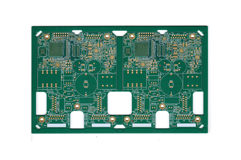
Explain some basic knowledge points of HDI circuit board in detail?
When talking about HDI circuit board, I believe most people are not very familiar with it, and their knowledge points are very unfamiliar with it. However, there is no need to worry. As a manufacturer, we will take this opportunity to talk about the basic information about HDI circuit board today. I hope you can bring some substantial help to you in the future.

First of all, whether you use an HDI board or buy it, you must have basic information about it. In this way, you will not be fooled by the sales staff, and you can also buy good quality products. In fact, HDI circuit board is a high-density interconnect manufacturing is a fast-growing field in the printed circuit board industry. The product has an inner line and an outer line. When in use, it is mainly used to use drilling, in-hole metallization and other processes to connect the internal lines of each layer. These are important points related to HDI circuit boards. In general, HDI circuit boards are mainly manufactured by the lamination method during production. The more the number of laminations, the higher the technical grade of the board. And ordinary HDI board is basically a layer, so there must be a difference between the two before. And high-order HDI adopts 2 or more times of lamination technology, and at the same time adopts advanced PCB technology such as stacking holes, electroplating filling holes, and laser direct drilling. Our company happens to be a professional manufacturer, if you need it, you can come here to order HDI circuit boards suitable for you. After all, this is a professional manufacturer, so the price of our equipment is also very reasonable.
After understanding what an HDI circuit board is and how it works, let's look at other information. In fact, this HDI circuit board has many advantages. For example, when in use, it can also increase the line density, the interconnection between the traditional circuit board and the parts. In addition, the cost of PCB can be reduced. When the density of PCB increases by more than eight layers, HDI will be manufactured at a lower cost than the traditional complex lamination process. HDI circuit board has many advantages, but also in other places. For example, it has better electrical performance and correct signals. This is conducive to the use of advanced construction technology. Thermal properties can be improved. Reliability is better. In short, no matter what, our products have advantages, and the quality is guaranteed when they are used. If necessary, please come and have a look. Has been with good quality and competitive prices for our customers to provide high-quality services, after nearly 20 years of continuous learning, in the stability of the continuous development and growth, has become one of the domestic influential HDI circuit board manufacturers.
After the introduction of the above content, we also have a certain understanding of HDI circuit board. If you are not clear, you can read the content of the article carefully. The next issue will bring more wonderful knowledge points. Today's information will be mentioned here first, hoping to bring help to relevant people.
HDI Board
Previous Page
The circuit board factory talks about the application advantage analysis of FPC in wearable devices.
2023-07-28
The FPC mentioned by the editor of the circuit board factory has excellent performance and plays an indispensable role in electronic products, meeting the development needs of smart phones and smart wearable devices. With the trend of miniaturization and thinning of electronic products, the consumption of FPC flexible circuit boards is increasing and booming.
Multi-layer circuit board factory-multi-layer circuit board compatible design points description.
2023-07-28
Most electronic products are inseparable from the component is multilayer circuit board, and the production quality of multilayer circuit board factory directly determines the use of electronic equipment and the use of quality, there are many points in the circuit board processing related to the compatibility of multilayer circuit board, and then affect the quality of the circuit board. What are the main points of the compatibility design of multilayer circuit boards under the popular science?_multilayer circuit board_multilayer circuit board factory_blind buried hole circuit board_HDI board proofing
2023-07-28
In the graphic electroplating process method of multi-layer circuit board factory, because the circuit pattern is easy to produce side etching in the etching process, the tin-lead alloy plating part is in the air and produces a suspension layer, which is easy to fall off, resulting in a short circuit caused by bridging between wires. Multilayer circuit board factory uses infrared hot melt process method, can make the exposed copper surface get very good protection. However, when it is used for infrared thermal melting of multi-layer circuit boards, the phenomenon of delamination and foaming between layers of multi-layer circuit boards is very serious due to high temperature, resulting in a very low yield of multi-layer circuit boards. _Blind buried hole circuit board_multilayer circuit board
2023-07-28
Before designing multilayer circuit boards, the multilayer circuit board structure must be determined according to the circuit scale, circuit board size and electromagnetic compatibility (EMC) requirements. That is to decide whether to use a 4-layer, 6-layer or higher multilayer circuit board. Once the number of layers is determined, the multilayer circuit board factory has decided to determine the placement of the electrical layers in the multilayer circuit board and how to distribute different signals on these layers. This is the choice of multilayer circuit board factory laminated structure.


