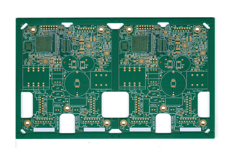
Take you through the basic overview of HDI boards?
With the increasing utilization rate of HDI circuit boards, there are many types on the market now. Although it is used in many industries, it is still very strange to most readers. As manufacturers, it is also necessary for us to give a detailed description here. If you want to know, come and have a look.

HDI circuit board is also a product often used in major industries. In fact, we still need to know a lot of information before using it. This HDI circuit board is a fast-growing field in the circuit board industry. According to our understanding, we found that 36 large customer servers with sequentially laminated multi-layer printed boards and stacked micro vias are now used, and the HDI circuit board we are talking about today is used here. Of course, it brings more benefits when it is used. For example, the current HDI circuit board technology is undoubtedly the future PCB architecture. Large ASICs and FPGAs with smaller device pitches, more I/O pins, and more embedded passive devices have increasingly shorter rise times and higher frequencies, and these basic information will be known when you see it in the future. It happens that Shenzhen Hengke Sheng Electronics Co., Ltd. is a professional R & D and production enterprise. If your industry needs it, you can come here to buy it to ensure that you will not be disappointed. Any knowledge about it can also come to consult us.
After knowing what an HDI circuit board is, let's take a look at some other knowledge points. The characteristics of this HDI circuit board are also very clear. For example, it is relatively simple to operate, and it has many functions after continuous completion. HDI circuit board it in imaging, such design requires a ring width of less than 75cm, in some cases even less than 50cm. These inevitably lead to low yields due to alignment problems. In addition, what we need to know when we use it is driven by miniaturization, and the wiring and spacing are getting finer and finer-meeting this challenge requires changing traditional imaging methods. Therefore, at this time, panel imaging can be performed in several steps by reducing the panel size or by using a shutter exposure machine. Therefore, the staff here must know that in fact, these two methods are to reduce the impact of material deformation to get a better alignment. Changing the panel size results in a high cost of materials, and the use of a shutter exposure machine results in a low throughput per day. Now enter the HDI circuit board company website, you can see our basic information, whether it is the company's establishment time or product display, as well as product specifications, can be seen on the official website.
After the introduction of the above content, we also learned some basic information about this HDI circuit board, so we won't feel strange when we see him again. Well, today's content will be here first, hoping to bring help to relevant people, but also bring more wonderful content.
HDI Board
The circuit board factory talks about the application advantage analysis of FPC in wearable devices.
2023-07-28
The FPC mentioned by the editor of the circuit board factory has excellent performance and plays an indispensable role in electronic products, meeting the development needs of smart phones and smart wearable devices. With the trend of miniaturization and thinning of electronic products, the consumption of FPC flexible circuit boards is increasing and booming.
Multi-layer circuit board factory-multi-layer circuit board compatible design points description.
2023-07-28
Most electronic products are inseparable from the component is multilayer circuit board, and the production quality of multilayer circuit board factory directly determines the use of electronic equipment and the use of quality, there are many points in the circuit board processing related to the compatibility of multilayer circuit board, and then affect the quality of the circuit board. What are the main points of the compatibility design of multilayer circuit boards under the popular science?_multilayer circuit board_multilayer circuit board factory_blind buried hole circuit board_HDI board proofing
2023-07-28
In the graphic electroplating process method of multi-layer circuit board factory, because the circuit pattern is easy to produce side etching in the etching process, the tin-lead alloy plating part is in the air and produces a suspension layer, which is easy to fall off, resulting in a short circuit caused by bridging between wires. Multilayer circuit board factory uses infrared hot melt process method, can make the exposed copper surface get very good protection. However, when it is used for infrared thermal melting of multi-layer circuit boards, the phenomenon of delamination and foaming between layers of multi-layer circuit boards is very serious due to high temperature, resulting in a very low yield of multi-layer circuit boards. _Blind buried hole circuit board_multilayer circuit board
2023-07-28
Before designing multilayer circuit boards, the multilayer circuit board structure must be determined according to the circuit scale, circuit board size and electromagnetic compatibility (EMC) requirements. That is to decide whether to use a 4-layer, 6-layer or higher multilayer circuit board. Once the number of layers is determined, the multilayer circuit board factory has decided to determine the placement of the electrical layers in the multilayer circuit board and how to distribute different signals on these layers. This is the choice of multilayer circuit board factory laminated structure.


