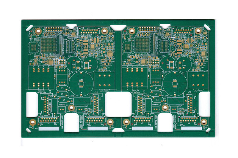
What is HDI circuit board? What are the advantages of HDI circuit board
With the development of science and technology, electronic design is constantly improving the performance of the whole machine, while also working hard to reduce the size. From mobile phones to smart weapons, "small" is the constant pursuit. High-density integration (HDI) technology enables smaller end-product designs while meeting higher electronic performance and efficiency standards. HDI circuit boards are widely used in mobile phones, digital cameras, MP3, MP4, notebook computers, automotive electronics and other digital products, among which mobile phones are widely used.

1. HDI Circuit Board Introduction
HDI is the English abbreviation of High Density Interconnector, that is, high density interconnect board, which is a circuit board with high wire distribution density using micro blind buried hole technology. High density interconnect (HDI) manufacturing is a fast growing area in the printed circuit board industry. From the first 32-bit computer introduced by HP in 1985 to the large customer server using 36 sequentially laminated multi-layer printed boards and stacked micro-vias, HDI/micro-via technology is undoubtedly the future PCB architecture. Smaller device pitch, I/O pins and embedded passive devices more large ASICs and FPGAs with increasingly shorter rise times and higher frequencies, they all require smaller PCB feature sizes, which drives the strong demand for HDI/micro vias.
2. HDI circuit board knowledge introduction
HDI circuit board has an inner layer and an outer layer, and then through drilling, hole metallization and other processes, each layer of circuit can be internally connected. Generally, the lamination method is adopted. The more the number of laminations, the higher the technical grade of the plate. The ordinary HDI circuit board is basically laminated once, and the high-order HDI circuit board adopts two or more lamination processes. At the same time, it adopts advanced PCB technologies such as stacking holes, electroplating filling holes, and laser direct drilling.
Advantages of 3. HDI circuit boards
1. Increase line density and interconnect traditional circuit boards with parts.
2. Can reduce the cost of PCB. When the density of the PCB is increased to more than eight layers, the cost of manufacturing it with HDI will be lower than the traditional complex pressing process.
3. Has better electrical performance and signal correctness. High assembly accuracy, small size, light weight, to meet the light and small electronic equipment.
4. It is conducive to the use of advanced packaging technology and mechanized, automated production, improve labor productivity, reduce the cost of electronic equipment.
5. It can improve thermal performance. Due to the high assembly density, the wiring of all parts (including components) is reduced, so the installation is simple and the reliability is high.
6. Good reliability, design can be standardized, which is conducive to intercommunication.
7. It can improve radio frequency interference/electromagnetic wave interference/electrostatic discharge (RFI/EMI/ESD)
8. Improve design efficiency. The shielding layer of the circuit and the magnetic circuit can be set, and the core heat dissipation layer can also be set to meet the needs of various special functions such as shielding and heat dissipation. These are the advantages of HDI circuit boards compiled by
and above. Hope to help you.
HDI Board
The circuit board factory talks about the application advantage analysis of FPC in wearable devices.
2023-07-28
The FPC mentioned by the editor of the circuit board factory has excellent performance and plays an indispensable role in electronic products, meeting the development needs of smart phones and smart wearable devices. With the trend of miniaturization and thinning of electronic products, the consumption of FPC flexible circuit boards is increasing and booming.
Multi-layer circuit board factory-multi-layer circuit board compatible design points description.
2023-07-28
Most electronic products are inseparable from the component is multilayer circuit board, and the production quality of multilayer circuit board factory directly determines the use of electronic equipment and the use of quality, there are many points in the circuit board processing related to the compatibility of multilayer circuit board, and then affect the quality of the circuit board. What are the main points of the compatibility design of multilayer circuit boards under the popular science?_multilayer circuit board_multilayer circuit board factory_blind buried hole circuit board_HDI board proofing
2023-07-28
In the graphic electroplating process method of multi-layer circuit board factory, because the circuit pattern is easy to produce side etching in the etching process, the tin-lead alloy plating part is in the air and produces a suspension layer, which is easy to fall off, resulting in a short circuit caused by bridging between wires. Multilayer circuit board factory uses infrared hot melt process method, can make the exposed copper surface get very good protection. However, when it is used for infrared thermal melting of multi-layer circuit boards, the phenomenon of delamination and foaming between layers of multi-layer circuit boards is very serious due to high temperature, resulting in a very low yield of multi-layer circuit boards. _Blind buried hole circuit board_multilayer circuit board
2023-07-28
Before designing multilayer circuit boards, the multilayer circuit board structure must be determined according to the circuit scale, circuit board size and electromagnetic compatibility (EMC) requirements. That is to decide whether to use a 4-layer, 6-layer or higher multilayer circuit board. Once the number of layers is determined, the multilayer circuit board factory has decided to determine the placement of the electrical layers in the multilayer circuit board and how to distribute different signals on these layers. This is the choice of multilayer circuit board factory laminated structure.


