Want to know about HDI circuit board and its advantages, there are all here!
HDI stands for High Density Interconnect, a technology that is rapidly gaining popularity in printed circuit boards. Overall, HDI boards can bring a range of benefits to technology. After all, they help simplify circuit boards, allowing them to do more while taking up less space. This means that the circuit board is smaller and the electronic device using such a circuit board is smaller. They can perform well, pack small, and be streamlined. Consider how many different types of devices have become smaller and smaller over the past decade. One reason is the use of HDI boards.

What is an HDI board?
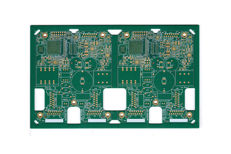
These boards can provide a large number of interconnections in a small space. The location on the component board is closer, which helps reduce the size, but the function is the same as the larger board. If the board has 120 to 160 pins per square inch, then it is an HDI board. When using general wiring, components are placed together. These types of plates are made possible by means of micro-hole technology and embedded blind holes. They are very efficient and are becoming more and more popular in various industries, as shown in the figure below.
Advantages of HDI boards
Many people want to find ways to reduce product yield. One of the best ways is to use HDI boards. They are a good solution when you need to reduce size and weight, and still need the functionality and reliability of the product. Another advantage of these circuit boards is the use of in-pad soldering and blind via technology. This allows the components to be put together, thereby reducing the length of the signal paths, which helps provide faster and more reliable signals because these paths are shorter.
Even though these motherboards can provide many advantages, you will find that they are still very affordable. This is a cost-effective solution for those who are looking for a reliable and durable electronic device. However, to determine if they are the right choice for you, it is important to learn more about them and how to use them. You also need to know the difference between a conventional PCB and an HDI board.
Where is the HDI circuit board now?
Due to the advantages provided by the HDI circuit board, you will find that it has been widely used in various electronic devices in many different industries. The medical industry is one of the famous industries. Medical devices manufactured today often need to be smaller. Whether it is a piece of equipment or an implant in the laboratory, a smaller size is often a better choice, and HDI boards can be of great help in this regard.
Many types of monitoring and detection equipment (such as endoscopes or colonoscopes) use this technology. Again, in these cases, the smaller the better. In addition to healthcare, HDI boards are also used in the automotive industry. To help make the most of the available space in the car, some electronic components are being made smaller. Of course, the same is true for tablets and smartphones, which is why many of these devices are getting thinner and thinner as they grow.
HDI Board
The circuit board factory talks about the application advantage analysis of FPC in wearable devices.
2023-07-28
The FPC mentioned by the editor of the circuit board factory has excellent performance and plays an indispensable role in electronic products, meeting the development needs of smart phones and smart wearable devices. With the trend of miniaturization and thinning of electronic products, the consumption of FPC flexible circuit boards is increasing and booming.
Multi-layer circuit board factory-multi-layer circuit board compatible design points description.
2023-07-28
Most electronic products are inseparable from the component is multilayer circuit board, and the production quality of multilayer circuit board factory directly determines the use of electronic equipment and the use of quality, there are many points in the circuit board processing related to the compatibility of multilayer circuit board, and then affect the quality of the circuit board. What are the main points of the compatibility design of multilayer circuit boards under the popular science?_multilayer circuit board_multilayer circuit board factory_blind buried hole circuit board_HDI board proofing
2023-07-28
In the graphic electroplating process method of multi-layer circuit board factory, because the circuit pattern is easy to produce side etching in the etching process, the tin-lead alloy plating part is in the air and produces a suspension layer, which is easy to fall off, resulting in a short circuit caused by bridging between wires. Multilayer circuit board factory uses infrared hot melt process method, can make the exposed copper surface get very good protection. However, when it is used for infrared thermal melting of multi-layer circuit boards, the phenomenon of delamination and foaming between layers of multi-layer circuit boards is very serious due to high temperature, resulting in a very low yield of multi-layer circuit boards. _Blind buried hole circuit board_multilayer circuit board
2023-07-28
Before designing multilayer circuit boards, the multilayer circuit board structure must be determined according to the circuit scale, circuit board size and electromagnetic compatibility (EMC) requirements. That is to decide whether to use a 4-layer, 6-layer or higher multilayer circuit board. Once the number of layers is determined, the multilayer circuit board factory has decided to determine the placement of the electrical layers in the multilayer circuit board and how to distribute different signals on these layers. This is the choice of multilayer circuit board factory laminated structure.


