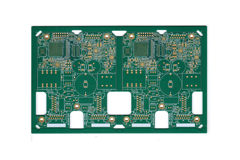
One minute to teach you how to distinguish between HDI circuit board and ordinary PCB
HDI circuit board is a high-density interconnection board, which is a circuit board with high line distribution density using micro-blind buried hole technology. The HDI circuit board has inner and outer circuits, and then through drilling, hole metallization and other processes, the circuits of each layer can be connected internally.

HDI boards are typically manufactured by a lamination process. The more times of lamination, the higher the technical level of the board. Ordinary HDI board is basically laminated once, high-order HDI adopts two or more lamination processes, and advanced PCB processes such as stacking holes, electroplating filling holes, laser straight drilling, etc.
When the density of the PCB is increased to more than eight layers, the cost of HDI will be lower than the traditional complex pressing process. HDI boards facilitate the use of advanced packaging technology, and their electrical performance and signal correctness are higher than traditional PCBs. In addition, the HDI board has better improvements in radio frequency interference, electromagnetic wave interference, electrostatic discharge, and heat conduction.
Electronic products continue to develop in the direction of high density and precision. The so-called "high" not only improves the performance of the machine, but also reduces the volume of the machine. High-density integration (HDI) technology can enable smaller end-product designs while meeting higher electronic performance and efficiency standards. At present, many popular electronic products, such as mobile phones, digital cameras, notebook computers, automotive electronics, etc., use HDI boards. With the upgrading of electronic products and market demand, the development of HDI circuit boards will be very rapid.
PCB(PrintedCircuitBoard), the Chinese name is printed circuit board. It is an important electronic component, a support for electronic components, and a carrier for electrical connection of electronic components. Because it is made of electronic printing, it is called "printed" circuit board. The main function of
is that after the electronic equipment adopts the printed circuit board, due to the consistency of similar printed circuit boards, manual wiring errors can be avoided, and the automatic insertion or installation, automatic welding and detection of electronic components can be realized, so as to ensure the quality of electronic equipment, improve labor productivity, reduce costs and facilitate maintenance.
PCB boards with blind buried holes are called HDI circuit boards? HDI circuit board is a high-density interconnection circuit board. The boards plated with blind holes and pressed are all HDI boards, which are divided into 1. 2. 3. 4. fifth-order HDI. Simple buried holes are not necessarily HDI.
The difference between HDI circuit board and ordinary PCB
The common PCB board is mainly FR-4, made of epoxy resin and electronic grade glass cloth. In general, traditional HDI uses adhesive-backed copper foil on the outer surface. Because the laser drilling through the glass cloth, so the general use of glass fiber-free adhesive copper foil. But now the high-energy laser drilling machine can already penetrate the 1180 glass cloth. In this way, there is no difference between ordinary materials.
The above is the content introduced by the editor on how to distinguish HDI circuit boards from ordinary PCBs. I hope it will be helpful to everyone,
HDI Board
The circuit board factory talks about the application advantage analysis of FPC in wearable devices.
2023-07-28
The FPC mentioned by the editor of the circuit board factory has excellent performance and plays an indispensable role in electronic products, meeting the development needs of smart phones and smart wearable devices. With the trend of miniaturization and thinning of electronic products, the consumption of FPC flexible circuit boards is increasing and booming.
Multi-layer circuit board factory-multi-layer circuit board compatible design points description.
2023-07-28
Most electronic products are inseparable from the component is multilayer circuit board, and the production quality of multilayer circuit board factory directly determines the use of electronic equipment and the use of quality, there are many points in the circuit board processing related to the compatibility of multilayer circuit board, and then affect the quality of the circuit board. What are the main points of the compatibility design of multilayer circuit boards under the popular science?_multilayer circuit board_multilayer circuit board factory_blind buried hole circuit board_HDI board proofing
2023-07-28
In the graphic electroplating process method of multi-layer circuit board factory, because the circuit pattern is easy to produce side etching in the etching process, the tin-lead alloy plating part is in the air and produces a suspension layer, which is easy to fall off, resulting in a short circuit caused by bridging between wires. Multilayer circuit board factory uses infrared hot melt process method, can make the exposed copper surface get very good protection. However, when it is used for infrared thermal melting of multi-layer circuit boards, the phenomenon of delamination and foaming between layers of multi-layer circuit boards is very serious due to high temperature, resulting in a very low yield of multi-layer circuit boards. _Blind buried hole circuit board_multilayer circuit board
2023-07-28
Before designing multilayer circuit boards, the multilayer circuit board structure must be determined according to the circuit scale, circuit board size and electromagnetic compatibility (EMC) requirements. That is to decide whether to use a 4-layer, 6-layer or higher multilayer circuit board. Once the number of layers is determined, the multilayer circuit board factory has decided to determine the placement of the electrical layers in the multilayer circuit board and how to distribute different signals on these layers. This is the choice of multilayer circuit board factory laminated structure.


