


This article takes you to know HDI board proofing
In today's safe and convenient living conditions, many new products have been produced accordingly. Today we will mainly talk about HDI board and HDI board proofing process.
HDI is the abbreviation of high density interconnection. At the same time, it is also a technology of printed circuit board. It is mainly based on a line of micro blind buried hole to distribute the circuit board with relatively high density. HDI is specially designed for small capacity users, because it is mainly compact products and adopts modular parallel design. In most cases, it adopts various patented technologies and digital signal processing technologies, and has strong short-term overload capacity and can adapt to load capacity on a global scale. The application of
HDI board has gradually expanded in recent years. It is generally manufactured by the lamination method. When the number of laminations is increased, the more advanced the technology of the plate, and the grade will be improved in turn. Ordinary HDI boards are basically single, while high-end HDI boards use 2 or more technologies. At the same time, technicians will also use other advanced technologies such as stacking holes and laser direct drilling. High-end HDI boards are mainly used in electronic devices such as mobile phones, advanced digital cameras, etc.
It has many advantages. For example, HDI board can present relatively low family planning electrical noise in improving product performance. Not only that, it can also minimize the structure of connecting holes and circuit branches, have a stable voltage path, be closer to the distribution of capacitance than other products, and even play a role in blocking radiation in specific environments.
But the HDI board also faces a new challenge, namely proofing technology. Due to the lack of professionals in its application technology and the lack of experienced knowledge in this industry, it is impossible to estimate the stacking status, price, drilling quantity and other issues at the beginning of the project design. At the same time, there are also certain challenges in the later assembly. How to reasonably select the structure is the key factor between the performance and cost of HDI board.
In the process of HDI board proofing , the selection of materials should also be fully considered. In most cases, the composition of HDI board proofing is generally resin, and some will also use improved acrylic resin, which mainly depends on its main application site and environment.
This article ends here today. I hope you have a deeper understanding of HDI board proofing after reading this article.
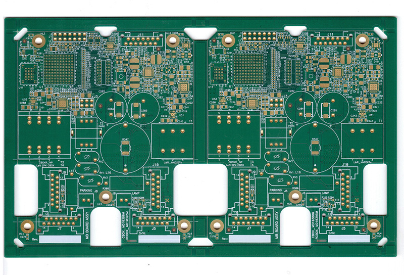
Proofing of HDI board
Next Page
The circuit board factory talks about the application advantage analysis of FPC in wearable devices.
2023-07-28
The FPC mentioned by the editor of the circuit board factory has excellent performance and plays an indispensable role in electronic products, meeting the development needs of smart phones and smart wearable devices. With the trend of miniaturization and thinning of electronic products, the consumption of FPC flexible circuit boards is increasing and booming.
Multi-layer circuit board factory-multi-layer circuit board compatible design points description.
2023-07-28
Most electronic products are inseparable from the component is multilayer circuit board, and the production quality of multilayer circuit board factory directly determines the use of electronic equipment and the use of quality, there are many points in the circuit board processing related to the compatibility of multilayer circuit board, and then affect the quality of the circuit board. What are the main points of the compatibility design of multilayer circuit boards under the popular science?_multilayer circuit board_multilayer circuit board factory_blind buried hole circuit board_HDI board proofing
2023-07-28
In the graphic electroplating process method of multi-layer circuit board factory, because the circuit pattern is easy to produce side etching in the etching process, the tin-lead alloy plating part is in the air and produces a suspension layer, which is easy to fall off, resulting in a short circuit caused by bridging between wires. Multilayer circuit board factory uses infrared hot melt process method, can make the exposed copper surface get very good protection. However, when it is used for infrared thermal melting of multi-layer circuit boards, the phenomenon of delamination and foaming between layers of multi-layer circuit boards is very serious due to high temperature, resulting in a very low yield of multi-layer circuit boards. _Blind buried hole circuit board_multilayer circuit board
2023-07-28
Before designing multilayer circuit boards, the multilayer circuit board structure must be determined according to the circuit scale, circuit board size and electromagnetic compatibility (EMC) requirements. That is to decide whether to use a 4-layer, 6-layer or higher multilayer circuit board. Once the number of layers is determined, the multilayer circuit board factory has decided to determine the placement of the electrical layers in the multilayer circuit board and how to distribute different signals on these layers. This is the choice of multilayer circuit board factory laminated structure.
National Service Hotline:
Shenzhen Hengke Sheng Electronics Co.
-
Fax: 86-755-27691537
Mailbox: csaa@hengkepcb.com
Website: www.hengkepcb.com
Address: No.253, Nanpu Road, Shajing Street, Baoan District, Shenzhen City, Guangdong Province
Copyright: Shenzhen Hengke Sheng Electronics Co., Ltd
Website Construction: China Enterprise Power Longgang