


What to prepare for HDI board proofing?
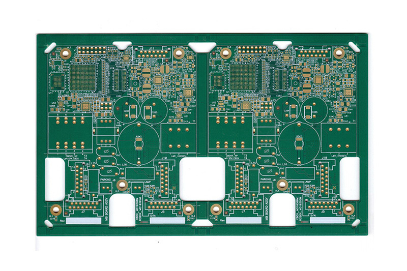
HDI board proofing ? What is HDI board? It is actually a high-density circuit board, which contains inner and outer circuits, and then uses drilling technology and in-hole metallization to process, so that the internal circuits of each layer can be connected to each other. Its appearance on the other hand is to increase the density of CPB, but HDI has a higher advantage than the latter.
in theHDI board proofing , first of all to make planning and design, do a good job of product system separation, this is a very important step. In the initial stages, the system segmentation of HDI panels, as its interconnection technology is constantly changing, will lead to many production challenges to be faced and solved, and it will be easier to take advantage of the benefits of HDI if product segmentation is carried out to translate the characteristics to system requirements and specifications. The next step is the layout of the HDI board. This includes balanced analysis and density requirements. As long as this step is properly deployed, the following HDI board proofing program will also reduce many unnecessary programs and reduce costs. Another thing that needs to be taken into account in the proofing process of HDI board is the wiring capacity, which refers to the length of the line that can be connected to all parts. There are three main factors that affect it, one is the line width spacing, reserved space, etc. This is the basis of the line graphics of each layer. The second is the matching of layers and buried holes, which should follow the established rules, in general, this step will be more complicated, which requires operators to have rich experience and theoretical knowledge in order to lay a good foundation for subsequent proofing. The third thing to pay attention to is efficiency, and the available area and percentage of use should be retained in the design.
After theHDI board proofing is completed, the production cost can be estimated more accurately by using auxiliary methods and evaluating density benefits. Under certain circumstances, it also helps to solve the problems that will occur in the later period, and can greatly increase the use effect of HDI so that it can play its real role. In the proofing also want to choose a good principle, in the vast majority of cases, technicians prefer to choose resin materials as the basis, because they have excellent adhesion, good heat resistance and appropriate conductive characteristics, coupled with relatively low cost, can reflect the high cost.
Proofing of HDI board
Previous Page
The circuit board factory talks about the application advantage analysis of FPC in wearable devices.
2023-07-28
The FPC mentioned by the editor of the circuit board factory has excellent performance and plays an indispensable role in electronic products, meeting the development needs of smart phones and smart wearable devices. With the trend of miniaturization and thinning of electronic products, the consumption of FPC flexible circuit boards is increasing and booming.
Multi-layer circuit board factory-multi-layer circuit board compatible design points description.
2023-07-28
Most electronic products are inseparable from the component is multilayer circuit board, and the production quality of multilayer circuit board factory directly determines the use of electronic equipment and the use of quality, there are many points in the circuit board processing related to the compatibility of multilayer circuit board, and then affect the quality of the circuit board. What are the main points of the compatibility design of multilayer circuit boards under the popular science?_multilayer circuit board_multilayer circuit board factory_blind buried hole circuit board_HDI board proofing
2023-07-28
In the graphic electroplating process method of multi-layer circuit board factory, because the circuit pattern is easy to produce side etching in the etching process, the tin-lead alloy plating part is in the air and produces a suspension layer, which is easy to fall off, resulting in a short circuit caused by bridging between wires. Multilayer circuit board factory uses infrared hot melt process method, can make the exposed copper surface get very good protection. However, when it is used for infrared thermal melting of multi-layer circuit boards, the phenomenon of delamination and foaming between layers of multi-layer circuit boards is very serious due to high temperature, resulting in a very low yield of multi-layer circuit boards. _Blind buried hole circuit board_multilayer circuit board
2023-07-28
Before designing multilayer circuit boards, the multilayer circuit board structure must be determined according to the circuit scale, circuit board size and electromagnetic compatibility (EMC) requirements. That is to decide whether to use a 4-layer, 6-layer or higher multilayer circuit board. Once the number of layers is determined, the multilayer circuit board factory has decided to determine the placement of the electrical layers in the multilayer circuit board and how to distribute different signals on these layers. This is the choice of multilayer circuit board factory laminated structure.
National Service Hotline:
Shenzhen Hengke Sheng Electronics Co.
-
Fax: 86-755-27691537
Mailbox: csaa@hengkepcb.com
Website: www.hengkepcb.com
Address: No.253, Nanpu Road, Shajing Street, Baoan District, Shenzhen City, Guangdong Province
Copyright: Shenzhen Hengke Sheng Electronics Co., Ltd
Website Construction: China Enterprise Power Longgang