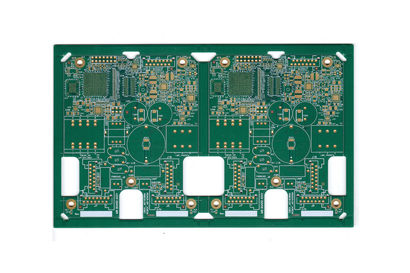
How is the copper thickness of the thick copper circuit board realized?
In the context of the increasing demand for industrial 4.0 to reduce costs and increase efficiency, industrial control has become a key solution to the problem. Under the industrial transformation, the traditional industrial automation control products are also expanding the territory and exploring new application fields. So, in the software can also control the copper thickness of thick copper circuit boards? Because there is no conventional operation, the thickness is not increased by software, customized to the manufacturer, there is a requirement to explain to the manufacturer. If you want to control the copper thickness of the thick copper circuit board, it is good to write down the requirements clearly and let the manufacturer control it according to your requirements. All you have to do is talk to the manufacturer of the board, but it seems that you don't want as much as you want, there is also an upper limit, which is as large as 100UM. The current intensity of

signal: When the average current of the signal is large, consider the current that the wiring width can carry. The line width can refer to the following data: the thickness of the copper foil in the PCB design, the relationship between the wiring width and the current. The current carrying capacity of copper foil for different thickness and width.
thick copper circuit board varies depending on the application and the current and thickness of the signal. How is the copper thickness of the thick copper circuit board realized?
The circuit board industry has no clear definition of the thick copper plate. General copper thickness of 2oz of the finished board called thick copper circuit board. Most circuit boards use 35um thick copper foil, which mainly depends on the application and the voltage/current of the signal. For PCB with excessive current, some will be 70um,105um, rarely 140um, etc.
thick copper circuit board copper thickness is how to achieve? Generally 2oz of finished copper is relatively thick, a manual printing screen is not enough to fill the gap between the line and the line, so to print twice solder mask.
So when making printed circuit boards, you will generally encounter a thickness of 2oz or more. When soldering, you will notice that thick copper plates require secondary screen printing. In order to achieve the effect that the line does not become red and the thickness of the solder resist layer on the surface of the line is greater than 10um.
The copper hole of the circuit board is not as thick as possible. All data needs to be done according to customer requirements. Customers can do as much as they want. Naturally, this cannot be completely consistent, but within the margin of error allowed by the customer. Copper plating generally has one copper and two copper. The main purpose of primary copper is to provide sufficient copper thickness for the second copper etching to ensure that the copper thickness after the second copper etching can meet the customer's standard requirements.
thick copper circuit board can generally be processed 6oz, 3oz, 2oz thick copper plate. Generally, multi-layer screen printing, multi-layer solder resist, and multi-layer copper sink are required to meet customer needs. The copper thickness of the thick copper circuit board is introduced here. Is it clear now?
thick copper circuit board
The circuit board factory talks about the application advantage analysis of FPC in wearable devices.
2023-07-28
The FPC mentioned by the editor of the circuit board factory has excellent performance and plays an indispensable role in electronic products, meeting the development needs of smart phones and smart wearable devices. With the trend of miniaturization and thinning of electronic products, the consumption of FPC flexible circuit boards is increasing and booming.
Multi-layer circuit board factory-multi-layer circuit board compatible design points description.
2023-07-28
Most electronic products are inseparable from the component is multilayer circuit board, and the production quality of multilayer circuit board factory directly determines the use of electronic equipment and the use of quality, there are many points in the circuit board processing related to the compatibility of multilayer circuit board, and then affect the quality of the circuit board. What are the main points of the compatibility design of multilayer circuit boards under the popular science?_multilayer circuit board_multilayer circuit board factory_blind buried hole circuit board_HDI board proofing
2023-07-28
In the graphic electroplating process method of multi-layer circuit board factory, because the circuit pattern is easy to produce side etching in the etching process, the tin-lead alloy plating part is in the air and produces a suspension layer, which is easy to fall off, resulting in a short circuit caused by bridging between wires. Multilayer circuit board factory uses infrared hot melt process method, can make the exposed copper surface get very good protection. However, when it is used for infrared thermal melting of multi-layer circuit boards, the phenomenon of delamination and foaming between layers of multi-layer circuit boards is very serious due to high temperature, resulting in a very low yield of multi-layer circuit boards. _Blind buried hole circuit board_multilayer circuit board
2023-07-28
Before designing multilayer circuit boards, the multilayer circuit board structure must be determined according to the circuit scale, circuit board size and electromagnetic compatibility (EMC) requirements. That is to decide whether to use a 4-layer, 6-layer or higher multilayer circuit board. Once the number of layers is determined, the multilayer circuit board factory has decided to determine the placement of the electrical layers in the multilayer circuit board and how to distribute different signals on these layers. This is the choice of multilayer circuit board factory laminated structure.


