


Multi-layer circuit board factory: multi-layer circuit board production process introduction
With more and more functions required by electronic products, the structure of multilayer circuit board is becoming more and more complex. Due to the space limitation of multi-layer circuit board , the circuit board is also gradually "evolution " from single layer to double layer and then to multi-layer. So what is so special about the manufacturing process of multilayer circuit board ?
Multilayer circuit board is a printed circuit board made of a conductive pattern layer and an insulator laminate. The number of layers of the conductive pattern is above 3 , and the interlayer electrical interconnection is realized through metallized holes. Double panels are the inner layer, two single panels are the outer layers, or two double panels are the inner layers. If two single panels are used as the outer layers, they are combined with each other through the layout system and insulating bonding materials, and According to the design requirements, the conductive patterns are connected together to become 4 layer, 6 layer printed circuit board, also known as multilayer PCB circuit board.
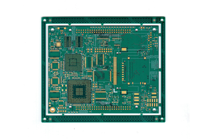
Multi-layer circuit board is generally made of epoxy glass cloth coated copper foil laminate, and its manufacturing process is developed on the basis of the starting double-layer board electroplating process. The general process of multi-layer circuit board is to etch and blacken first, then add a radius sheet according to the predetermined design, apply heating pressure of copper foil and pressure plate on the laminate and upper and lower surfaces respectively to obtain a "double-sided copper clad laminate " with prepared inner layer pattern, and then carry out numerical control drilling according to the predetermined positioning system. After drilling, the hole wall can be processed and decontaminated, and then the process of double-sided plated hole printed circuit board can be carried out.
multilayer circuit board, ceramic circuit board, circuit board factory, circuit board proofing, high frequency circuit board, multilayer circuit board factory, HDI circuit board
The circuit board factory talks about the application advantage analysis of FPC in wearable devices.
2023-07-28
The FPC mentioned by the editor of the circuit board factory has excellent performance and plays an indispensable role in electronic products, meeting the development needs of smart phones and smart wearable devices. With the trend of miniaturization and thinning of electronic products, the consumption of FPC flexible circuit boards is increasing and booming.
Multi-layer circuit board factory-multi-layer circuit board compatible design points description.
2023-07-28
Most electronic products are inseparable from the component is multilayer circuit board, and the production quality of multilayer circuit board factory directly determines the use of electronic equipment and the use of quality, there are many points in the circuit board processing related to the compatibility of multilayer circuit board, and then affect the quality of the circuit board. What are the main points of the compatibility design of multilayer circuit boards under the popular science?_multilayer circuit board_multilayer circuit board factory_blind buried hole circuit board_HDI board proofing
2023-07-28
In the graphic electroplating process method of multi-layer circuit board factory, because the circuit pattern is easy to produce side etching in the etching process, the tin-lead alloy plating part is in the air and produces a suspension layer, which is easy to fall off, resulting in a short circuit caused by bridging between wires. Multilayer circuit board factory uses infrared hot melt process method, can make the exposed copper surface get very good protection. However, when it is used for infrared thermal melting of multi-layer circuit boards, the phenomenon of delamination and foaming between layers of multi-layer circuit boards is very serious due to high temperature, resulting in a very low yield of multi-layer circuit boards. _Blind buried hole circuit board_multilayer circuit board
2023-07-28
Before designing multilayer circuit boards, the multilayer circuit board structure must be determined according to the circuit scale, circuit board size and electromagnetic compatibility (EMC) requirements. That is to decide whether to use a 4-layer, 6-layer or higher multilayer circuit board. Once the number of layers is determined, the multilayer circuit board factory has decided to determine the placement of the electrical layers in the multilayer circuit board and how to distribute different signals on these layers. This is the choice of multilayer circuit board factory laminated structure.
National Service Hotline:
Shenzhen Hengke Sheng Electronics Co.
-
Fax: 86-755-27691537
Mailbox: csaa@hengkepcb.com
Website: www.hengkepcb.com
Address: No.253, Nanpu Road, Shajing Street, Baoan District, Shenzhen City, Guangdong Province
Copyright: Shenzhen Hengke Sheng Electronics Co., Ltd
Website Construction: China Enterprise Power Longgang