


How does HDI PCB first-order and second-order and third-order distinguish?
The difference between the first order, the second order and the third order is to look at the number of laser holes. PCB core board is pressed several times and laser holes are punched several times, which is a few steps. That's the only difference.
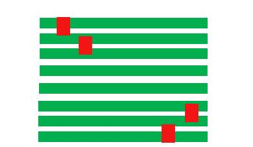
1. After pressing once, drilling = = = ", pressing copper foil again outside = = = ", laser drilling again, this is the first order, as shown in the following figure
2. After pressing once, drilling = = ", pressing copper foil again outside = = ", laser drilling again, drilling = = ", outer layer pressing again = copper foil =", laser drilling again. This is second order. The main thing is to see how many times you radiate, that is, how many orders.
The second order is divided into two types: stacked holes and bifurcation holes.
As shown in the following figure, there are eight layers of second-order stacked holes. The layers 3-6 are pressed together first, and the outer layers 2 and 7 are pressed together to make a laser hole. Laminate 1,8 again and make another laser hole. Is to make two laser holes. Because this kind of hole is superimposed, the process difficulty will be higher and the cost will be higher.

The following figure shows eight layers of second-order cross blind holes. This processing method is the same as the above eight layers of second-order stacked holes, and it also requires two laser holes. However, the laser holes are not stacked together, so the processing difficulty is much less.
The third order, the fourth order, and so on.
Expansion Data
HDI is an abbreviation of High Density Interconnection (High Density Interconnector ), which is a kind of (technology) for producing printed circuit boards and a circuit board with relatively high circuit distribution density using micro blind buried via technology. HDI is a compact product designed for small capacity users.
HDI Board
Next Page
Next Page
The circuit board factory talks about the application advantage analysis of FPC in wearable devices.
2023-07-28
The FPC mentioned by the editor of the circuit board factory has excellent performance and plays an indispensable role in electronic products, meeting the development needs of smart phones and smart wearable devices. With the trend of miniaturization and thinning of electronic products, the consumption of FPC flexible circuit boards is increasing and booming.
Multi-layer circuit board factory-multi-layer circuit board compatible design points description.
2023-07-28
Most electronic products are inseparable from the component is multilayer circuit board, and the production quality of multilayer circuit board factory directly determines the use of electronic equipment and the use of quality, there are many points in the circuit board processing related to the compatibility of multilayer circuit board, and then affect the quality of the circuit board. What are the main points of the compatibility design of multilayer circuit boards under the popular science?_multilayer circuit board_multilayer circuit board factory_blind buried hole circuit board_HDI board proofing
2023-07-28
In the graphic electroplating process method of multi-layer circuit board factory, because the circuit pattern is easy to produce side etching in the etching process, the tin-lead alloy plating part is in the air and produces a suspension layer, which is easy to fall off, resulting in a short circuit caused by bridging between wires. Multilayer circuit board factory uses infrared hot melt process method, can make the exposed copper surface get very good protection. However, when it is used for infrared thermal melting of multi-layer circuit boards, the phenomenon of delamination and foaming between layers of multi-layer circuit boards is very serious due to high temperature, resulting in a very low yield of multi-layer circuit boards. _Blind buried hole circuit board_multilayer circuit board
2023-07-28
Before designing multilayer circuit boards, the multilayer circuit board structure must be determined according to the circuit scale, circuit board size and electromagnetic compatibility (EMC) requirements. That is to decide whether to use a 4-layer, 6-layer or higher multilayer circuit board. Once the number of layers is determined, the multilayer circuit board factory has decided to determine the placement of the electrical layers in the multilayer circuit board and how to distribute different signals on these layers. This is the choice of multilayer circuit board factory laminated structure.
National Service Hotline:
Shenzhen Hengke Sheng Electronics Co.
-
Fax: 86-755-27691537
Mailbox: csaa@hengkepcb.com
Website: www.hengkepcb.com
Address: No.253, Nanpu Road, Shajing Street, Baoan District, Shenzhen City, Guangdong Province
Copyright: Shenzhen Hengke Sheng Electronics Co., Ltd
Website Construction: China Enterprise Power Longgang