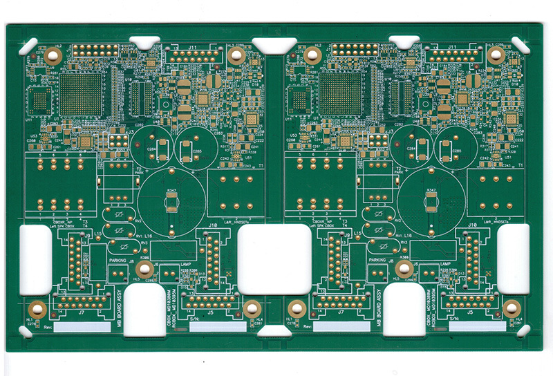
What is the thick copper circuit board? What is the role of thick copper circuit board?
There are many electronic engineers who cannot understand what the copper substrate is used for. The quality and reliability of the high thermal conductivity copper substrate is much better than that of the aluminum substrate and the iron substrate. The copper substrate is one of the most expensive metal substrates. The heat dissipation effect is many times better than that of the aluminum substrate and the iron substrate. It is suitable for high-frequency circuits, areas with large changes in high and low temperatures, and the heat dissipation and architectural decoration industries of communication equipment.

Printed Circuit Board (PCB) is usually bonded with a layer of copper foil on a glass epoxy board. The thickness of the copper foil is usually 18 μm, 35 μm, 55 μm and 70 μm. The usual thickness of the copper foil is 35 μm. The thickness of copper foil used in China is generally 35 ~ 50μm, and there are thinner than this, such as 10μm and 18μm; and thicker than this, such as 70μm. Thick copper circuit board is in the FR4 outer layer of bonding a layer of copper foil, when the completion of copper thick 2oz, defined as thick copper circuit board. PCB thick copper plate high temperature resistance, corrosion resistance, mainly used in products with power savings, especially the need to run a higher voltage and current of electronic products is the need for thick copper circuit board. The thicker the copper hole is, the better. All the data need to be made according to the customer's requirements. Thick copper circuit board has very good extension performance, not limited by the processing temperature, high melting point can be used oxygen blowing, low temperature is not brittle and other hot melt welding methods, and also fire, is a non-combustible material, its thickness is different, the specific application occasions are also very different.
thick copper circuit board because of the use and the thickness of the signal current. The finished circuit board with a copper thickness greater than or equal to 2OZ is called a thick copper plate, and the finished product with a copper thickness of 2OZ is thick. Hand screen printing once is not enough to fill the gap between the lines, need to print twice solder mask. When the material is 2OZ or thicker, the thick copper plate of the PCB will be noticed during solder resist, and secondary screen printing is required. In order to achieve the effect that the line does not become red and the thickness of the solder resist layer on the surface of the line is greater than 10um. Copper plating generally has one copper and two copper. The main purpose of primary copper is to provide sufficient copper thickness for the second copper etching to ensure that the copper thickness after the second copper etching can meet the customer's copper thickness standard requirements.
What is the role of thick copper circuit boards? With the continuous development of science and technology, people need high-performance, small-volume, multi-functional electronic products. In order to carry large current, reduce thermal strain, good heat dissipation, more and more electronic products. Industries that benefit from PCB thick copper plates include manufacturers of power supplies, automobiles, solar panels, and welding equipment. Thick copper wiring boards with copper plated vias are suitable for transferring heat to an external heat sink. Thick copper wiring boards are made by electroplating and etching techniques to increase the copper thickness of the through-hole and plated hole sidewalls.
thick copper circuit board
Previous Page
The circuit board factory talks about the application advantage analysis of FPC in wearable devices.
2023-07-28
The FPC mentioned by the editor of the circuit board factory has excellent performance and plays an indispensable role in electronic products, meeting the development needs of smart phones and smart wearable devices. With the trend of miniaturization and thinning of electronic products, the consumption of FPC flexible circuit boards is increasing and booming.
Multi-layer circuit board factory-multi-layer circuit board compatible design points description.
2023-07-28
Most electronic products are inseparable from the component is multilayer circuit board, and the production quality of multilayer circuit board factory directly determines the use of electronic equipment and the use of quality, there are many points in the circuit board processing related to the compatibility of multilayer circuit board, and then affect the quality of the circuit board. What are the main points of the compatibility design of multilayer circuit boards under the popular science?_multilayer circuit board_multilayer circuit board factory_blind buried hole circuit board_HDI board proofing
2023-07-28
In the graphic electroplating process method of multi-layer circuit board factory, because the circuit pattern is easy to produce side etching in the etching process, the tin-lead alloy plating part is in the air and produces a suspension layer, which is easy to fall off, resulting in a short circuit caused by bridging between wires. Multilayer circuit board factory uses infrared hot melt process method, can make the exposed copper surface get very good protection. However, when it is used for infrared thermal melting of multi-layer circuit boards, the phenomenon of delamination and foaming between layers of multi-layer circuit boards is very serious due to high temperature, resulting in a very low yield of multi-layer circuit boards. _Blind buried hole circuit board_multilayer circuit board
2023-07-28
Before designing multilayer circuit boards, the multilayer circuit board structure must be determined according to the circuit scale, circuit board size and electromagnetic compatibility (EMC) requirements. That is to decide whether to use a 4-layer, 6-layer or higher multilayer circuit board. Once the number of layers is determined, the multilayer circuit board factory has decided to determine the placement of the electrical layers in the multilayer circuit board and how to distribute different signals on these layers. This is the choice of multilayer circuit board factory laminated structure.


