


Multilayer Circuit Board Factory: Advantages and Applications of Multilayer Circuit Board
multi-layer circuit board is called multi-layer circuit board with more than two layers, such as 4 layer, 6 layer and 8 layer. Of course, there are also 3 layer or 5 layer circuit board designs, also known as multi-layer PCB circuit board.
Conductive traces larger than two layers are separated by insulating substrates between layers. After each layer of traces is printed, each layer of traces is laminated together. Then drilling is carried out to realize the conduction between the lines of each layer. The advantage of multi-layer circuit board is that the circuit can be distributed to multi-layer wiring, so as to design more precise products. Or smaller products, such as mobile phone circuit boards, small projectors, voice recorders and other bulky products, can be realized through multilayer boards. In addition, the use of multiple layers can be more flexible to control differential impedance, single-ended impedance and some signal frequency better output.
Multi-layer circuit board is the inevitable product of high-speed, multi-function, large-capacity and small-scale development of electronic technology. With the development of electronic technology, especially the widespread popularity of large-scale and ultra-large-scale integrated circuits, multi-layer printed circuits are rapidly developing in the direction of high density, high precision and high number of layers. Technologies such as fine lines, small aperture penetration, blind hole buried hole and high plate thickness aperture ratio have emerged to meet the needs of the market.
The reduction in the specifications of separate components and the rapid development of microelectronics, coupled with the requirements of the computer and aerospace industries for further increasing the packaging density of high-speed circuits, are continuously pushing electronic equipment to develop in the direction of forward volume reduction and mass reduction. Due to the limitation of available space, single-sided and double-sided printed boards have been unable to achieve further improvement in assembly density. Therefore, it is necessary to consider the use of printed circuits with more layers than the double-sided board, which creates conditions for the appearance of multilayer circuit board .
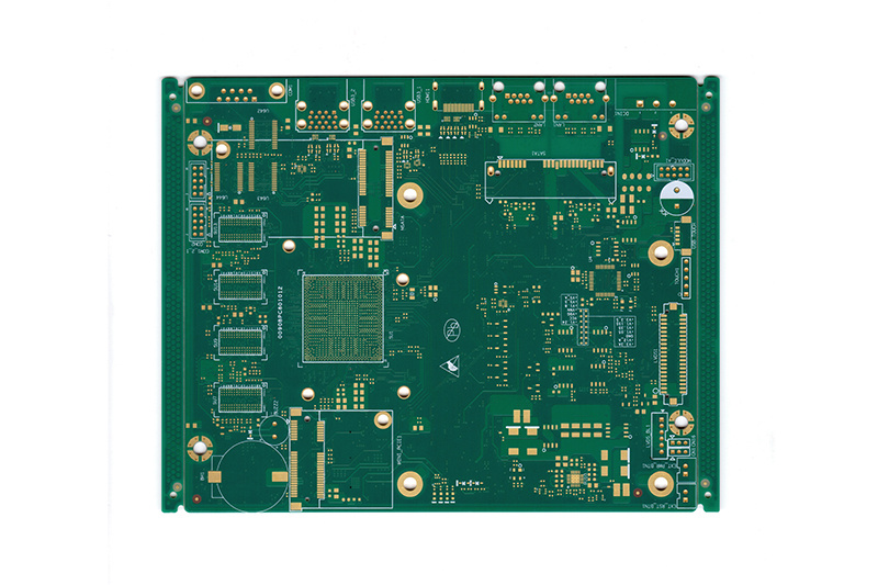
multilayer circuit board, multilayer circuit board, circuit board factory, multilayer circuit board factory
The circuit board factory talks about the application advantage analysis of FPC in wearable devices.
2023-07-28
The FPC mentioned by the editor of the circuit board factory has excellent performance and plays an indispensable role in electronic products, meeting the development needs of smart phones and smart wearable devices. With the trend of miniaturization and thinning of electronic products, the consumption of FPC flexible circuit boards is increasing and booming.
Multi-layer circuit board factory-multi-layer circuit board compatible design points description.
2023-07-28
Most electronic products are inseparable from the component is multilayer circuit board, and the production quality of multilayer circuit board factory directly determines the use of electronic equipment and the use of quality, there are many points in the circuit board processing related to the compatibility of multilayer circuit board, and then affect the quality of the circuit board. What are the main points of the compatibility design of multilayer circuit boards under the popular science?_multilayer circuit board_multilayer circuit board factory_blind buried hole circuit board_HDI board proofing
2023-07-28
In the graphic electroplating process method of multi-layer circuit board factory, because the circuit pattern is easy to produce side etching in the etching process, the tin-lead alloy plating part is in the air and produces a suspension layer, which is easy to fall off, resulting in a short circuit caused by bridging between wires. Multilayer circuit board factory uses infrared hot melt process method, can make the exposed copper surface get very good protection. However, when it is used for infrared thermal melting of multi-layer circuit boards, the phenomenon of delamination and foaming between layers of multi-layer circuit boards is very serious due to high temperature, resulting in a very low yield of multi-layer circuit boards. _Blind buried hole circuit board_multilayer circuit board
2023-07-28
Before designing multilayer circuit boards, the multilayer circuit board structure must be determined according to the circuit scale, circuit board size and electromagnetic compatibility (EMC) requirements. That is to decide whether to use a 4-layer, 6-layer or higher multilayer circuit board. Once the number of layers is determined, the multilayer circuit board factory has decided to determine the placement of the electrical layers in the multilayer circuit board and how to distribute different signals on these layers. This is the choice of multilayer circuit board factory laminated structure.
National Service Hotline:
Shenzhen Hengke Sheng Electronics Co.
-
Fax: 86-755-27691537
Mailbox: csaa@hengkepcb.com
Website: www.hengkepcb.com
Address: No.253, Nanpu Road, Shajing Street, Baoan District, Shenzhen City, Guangdong Province
Copyright: Shenzhen Hengke Sheng Electronics Co., Ltd
Website Construction: China Enterprise Power Longgang